Explanation of the general structure of a loading scheme
A 'pulse' (P) is one half of a wave (1) and a 'double pulse' (DP) is a full wave (2). It looks like this:
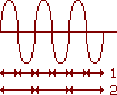
The physical structure of the data block is the following:
A block starts with a pilot signal. Upon detecting the pilot signal, the loading routine knows that soon the signal will transmit the stream of the data bits.
The pilot ends with some kind of synchronisation pulses, so that the loading routine can precisely detect the start of the data stream.
Usually the pilot consists of the series of equally length pulses and the synchronisation pulses are typically two distinctively shorter pulses.
After this, the bit stream immediately begins. Typically 1 bit of data is composed of 2 equal pulses (DP). The length of the pulses determines whether it's a '0' or a '1' bit.
Usually, a '1' bit pulse will be twice as long as a '0' bit pulse. The amplitude of each pulse is not important, as the loading routines are 'edge-triggered' rather than 'level-triggered'.
For the description of the schemes we use the notation:
P nnn = one pulse nnn T states long
DP nnn = double pulse, each pulse nnn T states long
nnnnx[] = repeat [] nnnn times
Sometimes we also add the word 'standard' to indicate that the values are identical to those used in the standard ROM loading scheme.
So the structure of the standard ROM loading scheme would be
PILOT 8063x[P 2168] (header) or 3223x[P 2168] (data)
SYNC standard P 667, P 735
DATA
bit 0 = DP 855
bit 1 = DP 1710
FLAG BYTE #00 (header), #FF (data)
PARITY BYTE present